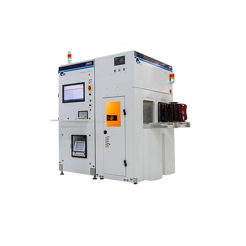
Automated 10nm particle deposition system for semiconductor wafers
Achieve precise 10 nm particle deposition on semiconductor wafers to enhance inspection accuracy and maintain high product yields effortlessly.
Deposits 10 nm Particles for Calibration
The Auto-Load 10 nm Particle Deposition System 2300G3A from TSI is a fully automated solution designed for semiconductor manufacturers and metrology labs. It uses advanced particle generation and Differential Mobility Analyzer (DMA) technology to accurately deposit PSL and SiO2 spheres as small as 10 nm onto 300 mm and 200 mm wafers. This precision ensures sub-nanometer repeatability and SI traceability, vital for defect inspection and tool calibration. The system supports 16 particle suspensions, offering versatility with a DMA-mode operating range of 10 nm to 2 µm. It features robotic wafer handling that processes up to 25 wafers per control job, significantly enhancing productivity. Ideal for wafer inspection, tool qualification, and particle classification, it seamlessly integrates into your production line with ergonomic design and worldwide support, setting a new standard in metrology applications.
Benefits
- Enhances inspection accuracy, leading to higher yield and quality.
- Increases productivity by processing up to 25 wafers per job with robotic automation.
- Ensures sub-nanometer repeatability for precise particle size control.
- Versatile application range from 10 nm to 2 µm accommodates varied calibration needs.
- Ergonomic design simplifies user operation and maintenance.
- Applications
- Particle deposition systems, Wafer inspection, Inspection tools calibration, Semiconductor manufacturing, Metrology applications
- End products
- 10 nm contamination standards, Film-coated wafers, Bare wafers, Defect inspection tools, Patterned wafers, Semiconductor wafers
- Steps before
- Wafer preparation, Particle suspension preparation
- Steps after
- Inspection tool calibration, Wafer inspection/qualification, Particle size analysis, Defect identification and classification
- Input ingredients
- PSL spheres, SiO2 spheres, particle suspensions
- Output ingredients
- 300 mm contamination standards, 200 mm contamination standards, deposited particles, bare wafer standards, film wafer standards, patterned wafer standards
- Market info
- Particle Size
- 10 nm to 2 µm
- Automation
- Fully automated
- Wafer Handling
- Robotic up to 25 wafers
- Particle Generation
- Nanoparticle atomization
- Size Classification
- DMA size classification
- Repeatability
- Sub-nanometer
- Traceability
- SI traceability
- Particle Suspension Capacity
- 16 particle suspensions
- Automation level
- Automated
- Batch vs. continuous operation
- Batch
- Cleaning method
- Automated Cleaning
- Recipe control
- Precise recipe control of particle size and deposition pattern
- Particle size control
- Sub-nanometer repeatability
- Density/particle size
- 0.5–2.5 g/cm³ / 10–100 nm
- Particle Material
- PSL and SiO2
- Wafer size compatibility
- 300 mm / 200 mm
- Robotic wafer handling capacity
- Up to 25 wafers
- Control job processing
- Single control job
- Automation level
- Fully automated
- Deposition pattern types
- Full (blanket), Spot, Arc, Ring
- Integration possibilities
- Robotic wafer handling
- Recipe control
- Automated recipe for calibration curve
- Deposit pattern
- Full, Spot, Arc, Ring