20 nm particle deposition system for semiconductors
Calibrate and qualify defect inspection tools with precision using a system that deposits 20 nm particles, enhancing wafer metrology and improving product yield.
Deposits 20 nm Particles for Calibration and Inspection
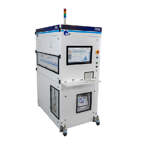
The Manual-Load 20 nm Particle Deposition System 2300G3M from TSI offers unparalleled precision in the deposition of nanoparticle size standards, notably for semiconductor and electronics metrology applications. Utilizing advanced particle generation with a Differential Mobility Analyzer (DMA) technology, it controls particle sizes with sub-nanometer repeatability, crucial for defect inspection and calibration in semiconductor manufacturing. This system supports a range of substrates, including 150 mm, 200 mm, and 300 mm wafers, facilitating various wafer metrology applications and enhancing product yield. With an operating range of 20 nm to 2 µm, it can handle up to 16 particle suspensions, allowing the production of diverse inspection tool calibration curves within a single automated recipe. The 2300G3M integrates seamlessly into existing production lines, offering manual batch operation suited for research and processing departments. It ensures clean particle generation and minimizes residue through precise atomization and size classification mechanisms. Designed with ergonomic considerations, it promises easy maintenance and reliable worldwide support.
Benefits
- Ensures precise calibration with sub-nanometer repeatability, improving inspection accuracy.
- Supports multiple wafer sizes, enhancing flexibility in semiconductor production.
- Minimizes particle residues, maintaining high-quality standards in metrology applications.
- Reduces tool recalibration frequency, optimizing production line uptime.
- Provides ergonomic design for ease of use and maintenance, increasing operational efficiency.
- Applications
- Wafer metrology, Film inspection, Inspection tool calibration, Process monitoring, Semiconductor manufacturing
- End products
- 20 nm psl spheres, 200 mm wafers, Semiconductor wafers, Sio2 spheres, Contamination standards, Process calibration curves, Film coatings, 150 mm wafers, 300 mm wafers
- Steps before
- Substrate preparation, Wafer cleaning, Calibration setup
- Steps after
- Inspection tool calibration, Wafer qualification, Defect inspection
- Input ingredients
- PSL spheres, SiO2 spheres, particle suspensions, 150 mm wafers, 200 mm wafers, 300 mm wafers
- Output ingredients
- deposited particles, nanoparticle depositions, calibrated defect inspection tools, high-quality contamination standards
- Market info
- Particle size range
- 20 nm to 2 µm
- Substrate sizes supported
- 150 mm, 200 mm, 300 mm wafers
- Particle deposition pattern
- Full, Spot, Arc, Ring
- Particle generation technology
- Nanoparticle atomization
- Size classification
- DMA technology
- Sample capacity
- 16 particle suspensions
- Repeatability
- Sub-nanometer repeatability
- Traceability
- SI traceability
- Automation level
- Manual loading
- Batch vs. continuous operation
- Batch
- Particle size control
- Sub-nanometer repeatability
- Mode operating range
- 20 nm to 2 µm
- Recipe control
- Automated recipe for deposition
- Deposit patterns
- Full, Spot, Arc, and Ring
- SiO2 Spheres
- Compatible
- Polymeric Spheres (PSL)
- Compatible
- Wafer Substrate Sizes
- 150 mm, 200 mm, 300 mm
- Density/particle size
- 20 nm to 2 µm
- ISO Certification
- ISO 9001 / ISO 14001
- Compact footprint
- N/A
- Control panel type
- Manual
- Discharge method
- Manual Loading
- Control panel type
- Ergonomic design
- Integration possibilities
- Worldwide service and support
- Flexible substrate handling
- 150 mm, 200 mm, 300 mm wafers
- Deposit pattern control
- Full, Spot, Arc, and Ring